The Young's Modulus of Silicon
A Simple Explanation
By M.A. Hopcroft, Ph.D.
Introduction
The value of the Young's modulus of silicon is often required for engineering designs using micro-electro-mechanical systems (MEMS) technology. However, silicon is an anisotropic crystalline material and so the answer to the question, "What is the Young's modulus of silicon?" is, "it depends, and it can vary by up to 45%". Fortunately, it is straightforward to determine the correct answer for any situation. A condensed answer to the question and explanation is given here.The information here has been published with significant additional material in a peer-reviewed journal. Please cite this reference when using this information:
M. A. Hopcroft, W. D. Nix, and T. W. Kenny, "What is the Young's Modulus of Silicon?", IEEE Journal of Microelectromechanical Systems, vol. 19, Issue 2, pp. 229-238, 2010 (DOI: 10.1109/JMEMS.2009.2039697).
Skip the explanation and go straight to the answer...
Crystal Orientation
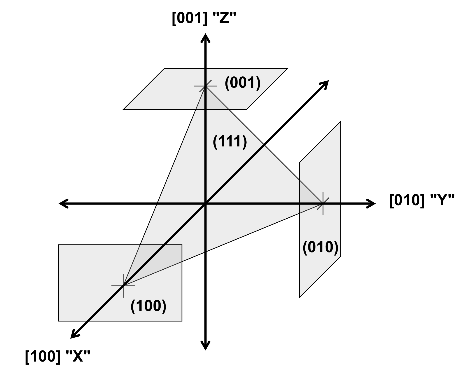
Silicon is an anisotropic crystalline material with cubic symmetry (Fig. 1). The orientation of crystal structures is described by Miller indices, which are integer groups such as “hkl”. The integer groups can describe a direction vector, indicated by square brackets ("[hkl]"), or a plane perpendicular to the direction, indicated by parentheses ("(hkl)"). The cubic crystal directions are shown in Figure 2. In a cubic crystal, directions separated by 90° are equivalent, and these "families" of equivalent directions are indicated by corner brackets ("<hkl>").
 |
 |
| Figure 1 - Silicon crystal structure | Figure 2 - Cubic crystal directions |
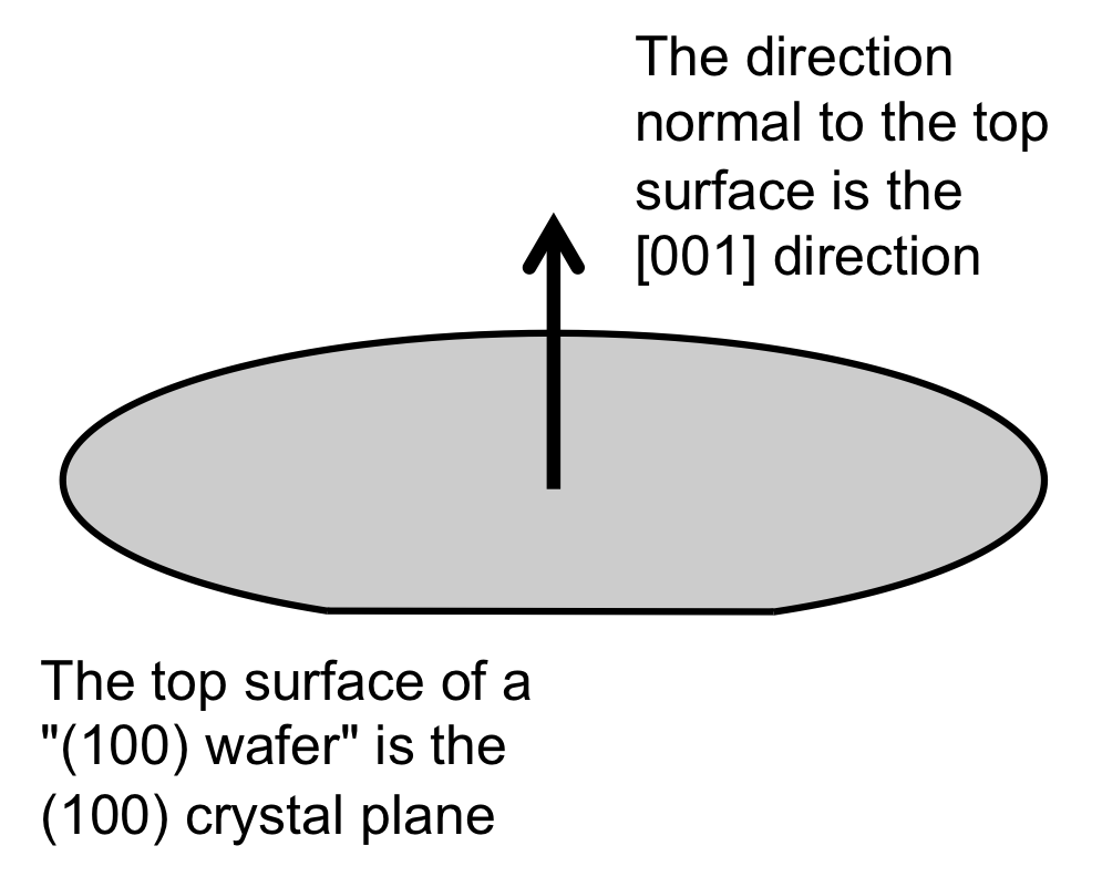
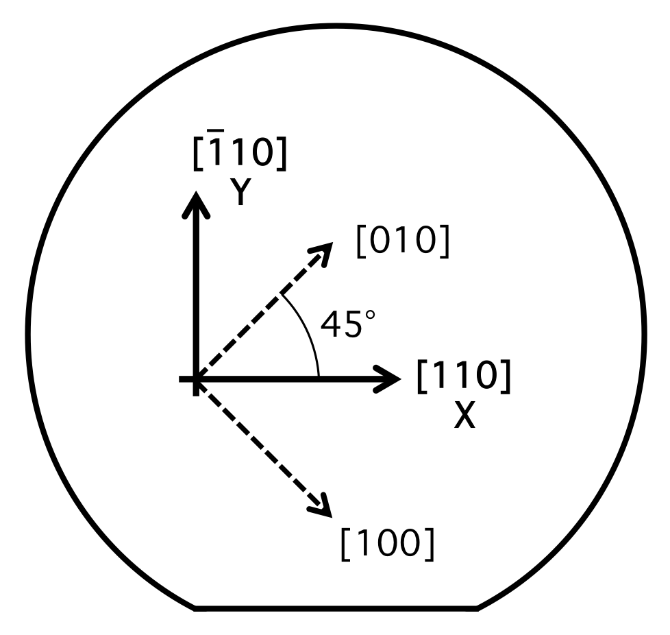
Silicon wafers are described by the crystal orientation of their surface and by the location of the wafer flats. The most common wafer type is called a "(100) wafer", meaning that the surface of the wafer is parallel to a (100) plane of the silicon in the wafer (Fig. 3). The major flat of these wafers is parallel to the <110> direction of the silicon crystal structure. Therefore, for a (100) silicon wafer, the "X" and "Y" directions most typically used in the layout of a MEMS design correspond the the <110> directions of the silicon crystal, as shown in Figure 4.
|
|
|
|
|
Anisotropic Elasticity
Hooke's law describes the linear, isotropic relationship between stress (σ) and strain (ε) using compliance (S) and stiffness (C):σ=Cε , or ε=Sσ .
The mechanical stiffness of materials under uniaxial loading is called the Young's modulus, and is typically represented by the symbol E in engineering texts, so Hooke's law is often written as σ=Eε .
Hooke's law can be extended to anisotropic materials with a tensor formulation that includes orientation:
σij=cijklεkl , or εij=sijklσkl .
The general case of a fourth-rank tensor requires 81 terms. Fortunately, due to the properties of cubic symmetry, the anisotropic properties of a cubic crystal can be described with a 6x6 matrix using simplfied tensor notation and only 3 independent values are required in this matrix. The values in this matrix are determined with respect to a specific set of XYZ axes. The mathematical convention for these matrix transforms is to use the "principal crystallographic axes", which for a cubic crystal are the <100> directions. Therefore, unless otherwise specified, values for the elasticity constants are for the <100> axes, not the <110> axes typically used in MEMS design.
The best values for the elastic constants for silicon from the scientific literature are given in Table 1.
| C: 109 Pa S: 10-12 Pa |
C11 | C12 | C44 | S11 | S12 | S44 |
| Silicon <100> | 165.6 | 63.9 | 79.5 | 7.68 | -2.14 | 12.6 |
Elasticity for Design Calculations
When doing design calculations, isotropic approximations are typically used, in order to make the calculation tractable. For an anisotropic material such as silicon, the correct value for the relevant crystal orientation must be used. For example, a silicon cantilever which is drawn parallel to the X axis in a MEMS layout tool for fabrication on a typical (100) silicon wafer would have its axis of bending in a <110> direction. Therefore, material properties for <110> should be used for design calculations, such as estimating the deflection of the cantilever. In this case, the appropriate value of E is 169 GPa. However, if the cantilever was fabricated "off-axis", aligned with a <100> direction, then the appropriate value of E for calculation is 130 GPa. The most common values of E used in design calculations are given in Table 2.| Load Case | Symbol | Appropriate E value | Axial stress/strain, incl. beam bending <110> directions ("X or Y axis") <100> directions ("45° off-axis") | E | 169 GPa 130 GPa |
| Plate bending, ν = 0.064 for <110> in (100) | E'110 | 170 GPa |
| Thin film biaxial stress/strain, (100) plane | B100 | 180 GPa |
| Shear load, twisting a <110> ("X" or "Y") beam | G | 50.9 GPa |
| Stress Concentrations | EV | 166 GPa |
| Hydrostatic loads (Bulk modulus) | B | 97.8 GPa |
| Temperature Coefficient of E | TCE | ~ -60 ppm/°C |
Elasticity for Finite Element Modeling
All modern finite element modeling (FEM) software has the capability to perform calculations using the anisotropic formulation of elasticity. The trick is to enter the appropriate values into the software. In some cases, the software will require the elastic constants in simplified tensor notation. In other cases, the user may be required to enter the elastic constants which have been transformed from the <100> axes to the to the axes of the silicon wafer crystal orientation. Refer to the documentation of your finite element software for details. The values for some common cases are given in Table 3.| Orthotropic stiffness values for (100) silicon wafers |
Ex = Ey = 169 GPa, Ez = 130 GPa νxz = νyz = 0.36, νzx = νzy = 0.28, νxy = νyx = 0.064 Gyz = Gzx = 79.6 GPa, Gxy = 50.9 GPa |
| Cubic stiffness matrix values (principal axes) |
C11 = C22 = C33 = 165.6 GPa C12 / 21 = C13 / 31 = C32 / 23 = 63.9 GPa C11 = C22 = C33 = 79.6 GPa |
| Cubic stiffness tensor values (principal axes) |
c1111 = c2222 = c3333 = 165.6 GPa c1122 = c1133 = 63.9 GPa c2211 = c2233 = 63.9 GPa c3311 = c3322 = 63.9 GPa c1313 = c3113 = c1331 = c3131 = 79.6 GPa c2323 = c3223 = c2332 = c3232 = 79.6 GPa c1212 = c2112 = c1221 = c2121 = 79.6 GPa |
Additional Notes
The elasticity values given here are correct for bulk silicon. Silicon structures with dimensions less than 100 nm will experience a significant reduction in E due to surface effects. For more information, see: Li, et al., "Ultrathin single-crystalline-silicon cantilever resonators...", Appl. Phys. Lett. 83, 3081 (2003).Elasticity values for poly-crystalline silicon ("polysilicon") can vary significantly with deposition methods and conditions. For estimation purposes, polysilicon can be treated isotropically, using Epoly = 160 GPa, νpoly = 0.22 .
The piezoresistive coeffients in silicon require an analogous analysis to the elasticity coefficients. See, for example, "Piezoresistor Design and Applications".
References
The material presented here is condensed from:M. A. Hopcroft, W. D. Nix, and T. W. Kenny, "What is the Young's Modulus of Silicon?", Journal of Microelectromechanical Systems, vol. 19, Issue 2, pp. 229-238, 2010 (DOI: 10.1109/JMEMS.2009.2039697).
A complete list of references is available in that paper. Some selected references are:
- "Foundations of MEMS",
2006
C. Liu
Book published by Pearson Education, Inc., Upper Saddle River, NJ
ISBN: 0-13-147286-0
- "Microsystem Design",
2001
S. D. Senturia
Book published by Kluwer Academic Publishers, Boston
ISBN: 0-7923-7246-8
- "Physical Properties of Crystals: Their Representation by Tensors and Matrices",
1985
J. F. Nye
Book published by Oxford University Press, Oxford
ISBN: 0198511655
- "Electronic effects in the constants of n-type silicon", 1967
J. J. Hall
Physical Review, 161, (3), pp. 756
- "Youngs' Modulus, Shear Modulus and Poisson's Ratio in Silicon and Germanium", 1965
J. J. Wortman and R. A. Evans
Journal of Applied Physics, 36, (1), pp. 153-156
- "Piezoresistor Design and Applications (Microsystems and Nanosystems)",
2013
J. C. Doll and B. L. Pruitt
Book published by Springer Publishing Co. New York
ISBN: 978-1461485162
Supported by Red Dog Research and our sponsors